Nurofen FeverSmart Temperature Monitor Teardown
The Nurofen FeverSmart Temperature Monitor is a wearable real-time temperature sensor for small children and babies, which adheres to the child’s skin under the armpit and provides real time measurements of temperature to a companion smartphone, via a base/relay station.
This was recently on sale at a significant discount (£14.99 vs RRP £49.99) at my local TK Maxx, and it appears Nurofen might have discontinued the product. Being interested in small bluetooth devices, I bought one to take apart.
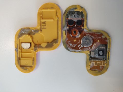
The sensor is shown on the left, and the base station (without lid) on the right. Not shown are the transparent stickers used to adhere the sensor on to the child, as I have given those away to someone else who is actually using the device.
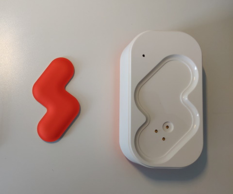
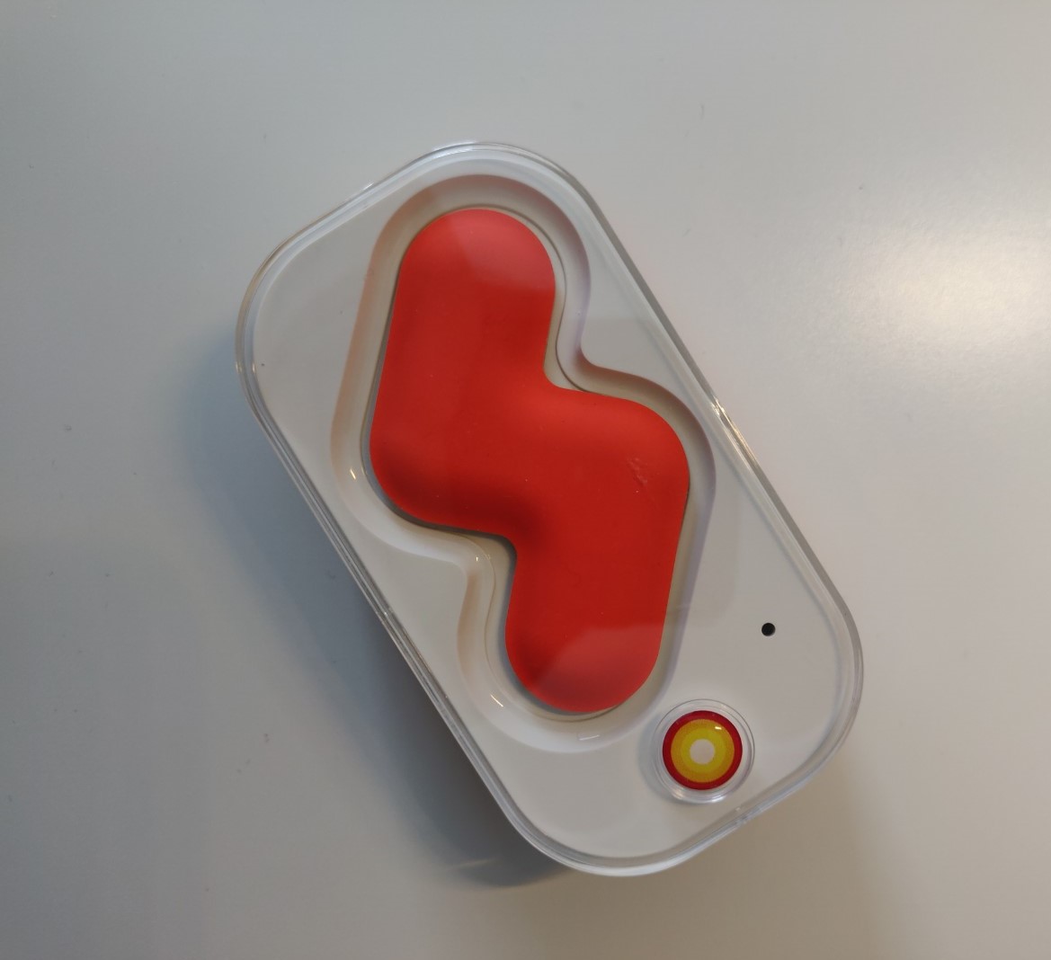
The sensor magnetically snaps to the base station, with a single white LED illuminating, changing to flashing when charged. Alignment seems good, I tried a few times and the sensor snaps into place reliably. A clear lid clips on to protect it when charging.
Base Station
The base station is responsible for both charging the sensor and “relaying” bluetooth communications from it. From the documentation:
The Base Station must be kept within 1.5m/4.5ft from the Monitor in order for it to boost the signal effectively
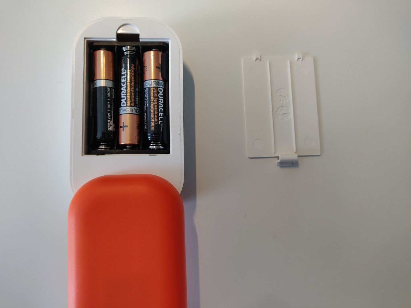
A swinging orange flap covers the back of the device. This is a nice smooth feeling plastic, and swivels round, snapping into place every 90 degrees. It allows for some storage of adhesive pads within the device, and a a more conventional flap covers the 3x AAA batteries within an off the shelf holder.
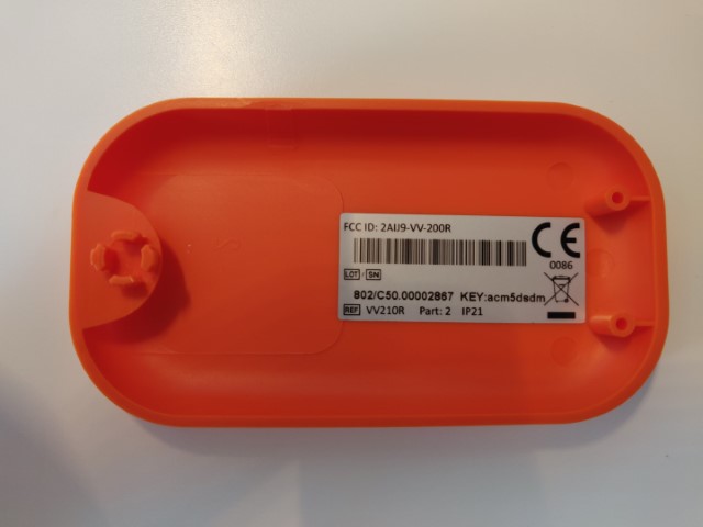
The FCC ID is visible on the inside of the lid, along with the pairing key, which is used within the app as an extra security measure. The ID can be checked on fccio.io to see the official internal photos. The use of a pairing key (presumably uniquely printed per device) instead of the usual “hold to pair” switch could be due to size limitations, concern over accidental pressing in use, or other usability issues.
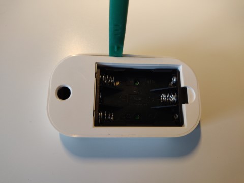
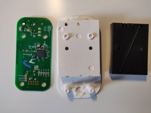
The orange back piece is simply pulled off, and then a plastic spudger quickly opens the case. Only four snap fits are present, one in the middle of each side, and no adhesive is used.
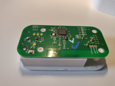
Once open, the single PCB can be seen. The off the shelf battery holder is soldered onto the main PCB by hand, and this holds the battery down and the PCB in. Nothing else holds the PCB and battery holder in apart from these two hand-soldered joints, which results in very fast assembly, with standoffs moulded into the case for alignment.
Unfortunately, the pads do not have any thermal relief, and so hand soldering these is difficult as the large ground plane quickly wicks away heat. The factory has tried to compensate with a higher wattage iron, and so the joint is poor quality without a proper fillet, and flux and solder spatter are spread around, including a gob of solder stuck in the soft epoxy top of the LED! Clearly, quality control for the electronics is sub-par to accept this level of spatter, as the large handwritten tick mark indicates that some visual inspection was performed. It is surprising that the factory would not ask for the PCB design to be changed to add thermal relief, which would be a very simple fix.
Base Station PCB Electronics
The base station PCB is a quite simple PCB, with single sided surface mount assembly for lowest assembly cost. Notably however, certain components have underfill added, which seems unusual as the durability requirements (temperature/vibration) for this product are quite low.
The silkscreen indicates the design was released on 29th of April 2016, and “Vivalink” is the name of the company from which Nurofen licensed the design.

- Yellow:Battery holder solder points
- Red: Unknown linear regulator
- Green: White Status LED
- Blue: TI CC2640 Bluetooth Low Energy MCU
- Purple: Switched coax connector
- Pink: Inverted-F antenna
- Orange: Debug header (not fitted)
Power is provided by the 3xAAA batteries in series at 4.5V, and is stepped down to a lower voltage (likely 3.0V) by the linear regulator U1, a very simple and low power1 approach.
The bluetooth MCU U1 is a midrange part, clocking in at $1.69 at 1K quantity. It has both a Cortex-M3 application processor and a dedicated Cortex-M0 for the bluetooth stack. Inductor L1 works with the DC/DC buck regulator to increase efficiency when the radio is active. The MCU is clocked by a high frequency crystal Y2 when it is awake, and the low frequency 32KHz Y1 when it is asleep. Since this is likely a high volume product, the extra certification expense of an IC over a module is probably justified.
The three test points are surface mount soldered, but rest in plated through holes to give some measure of reinforcement. No ESD protection is visible on the VDD pin, a possible cause of failure, but the “I/O” pin is possibly protected by D1/R2/R3. It is unknown what this pin is used for, some investigation with a scope is needed.
The antenna is an Inverted F type2, which offers better performance and resistance to detuning than the more common “folded” style, at the expense of greater board area. Note that the ground plane and components are kept out of the long axis of the antenna, which would be affected by nearby metal components3.
The matching network C5/C15 tunes the antenna for the application. A switched coaxial connector (purple) lies within the signal path, and disconnects the antenna when a test pin is connected during test/programming, so that the RF performance can be tested. When tuning the antenna, this connector can be placed in reverse orientation, so the bluetooth IC is disconnected and the antenna connected directly to a network analyser.
The through hole pads are for a full size 2.54mm pitch debug header, which is used during development. Test points TP5-TP10 would be used for programming during production, using TIs “cJTAG” interface. This is in contrast to the SWD interface that is more common when using ARM Cortex processors, but the total number of pins are approximately the same. Test point TP11-TP13 are likely for a UART used for both production test and for Direct Test Mode (DTM) in Bluetooth SIG qualification testing.
Sensor
The sensor is adhered to the skin using disposable adhesive pads, which have a small hole in to allow the single protruding contact to touch the skin directly, so heat flows through the contact pad to an internal temperature sensor. The sensor is rated to IP25, and is welded/glued completely shut.
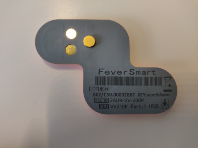
The key and FCC ID are printed on the underside. Notably, the internal photos filed with the FCC show a slightly different PCB layout.
On cutting the sensor open by running a scalpel around all edges, it can be seen that the top half is injection moulded separately before the unit is assembled, and overmoulding is not used. A very thin film/coating4 protects the components during this welding/gluing, and can be easily scratched off with a fingernail. It likely also serves to hold the two magnets in place, the two black circles at top right. Overmoulding is unlikely to have been suitable as it would run the risk of damage to the battery.
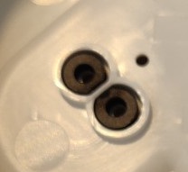
On closer inspection of the base station, two ring magnets are present around the charging pins, and attract the two magnets within the sensor on the opposite side of the contact pads, maximising the contact force.
Sensor Electronics
The sensor electronics are mounted on a rigid-flex PCB, allowing the sensor to provide a more comfortable curved fit. This method of PCB construction is one of the most expensive methods, but a pure flexible PCB would likely put excess stress on the solder joints and lead to failure. To further reinforce the rigid sections, a thin metal sheet is adhered to the underside of the PCB. The ground plane used in the flexible sections is hatched for flexibility.
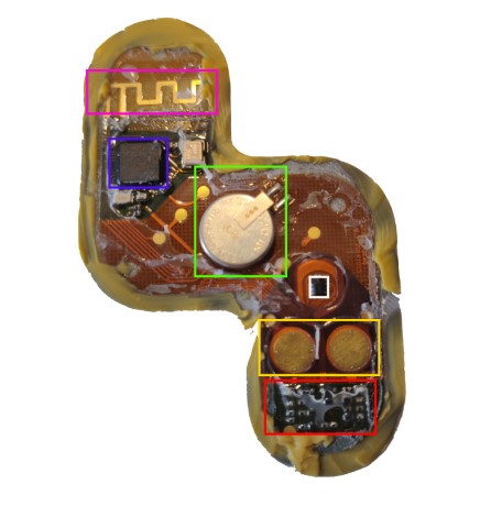
- Purple: Folded Monopole Antenna
- Blue: Dialog DA14580 Bluetooth Low Energy MCU
- Green: Seiko MS920SE-FL27E 3.0V 11mAh Li-Ion rechargeable battery
- Red: Discrete battery charger circuitry
- Yellow: Reverse side of contact pads, magnets are adhered to these.
- White: Unknown temperature sensor
The DA14580 is a quite cheap bluetooth microcontroller, using a single Cortex-M0 core running at 16MHz for both the application and the bluetooth stack. Rather than reprogrammable flash memory, it has 32kB of one time programmable (OTP) memory for user code, with the BLE stack stored in 84kB of ROM. The extra development costs of using two different manufacturers vs consolidating to one Bluetooth MCU supplier must have been justified by the expected cost savings of using this Dialog part.
The PCB trace antenna antenna is a small folded Inverted-F antenna. This would be very close to the skin when adhered, with only the thickness of the rubber and sticker beneath the device separating it. The degraded performance from this is likely responsible for the 1.5 meter range to the base station, along with the decreased output power needed for long battery life.
The temperature sensor is on the opposite side of the PCB from the protruding contact pad, a 6 pin leaded package5. The included instruction manual claims an accuracy of ±0.2°C from 35 to 42C, which is quite high without calibration. Looking at TIs website, only the TMP112 is a close fit at ±0.5°C (before calibration), and 6 pin package.
Analysis
The design seems quite robust, especially the sensor part. Other than some bad quality hand soldering, the general quality is good, with proper antenna design, good levels of reinforcement, and “name brand” parts.
Charging is fast and easily snaps together, with proper sprung pogo pin being used in the base station, and strong magnets ensuring a high contact force to adequately penetrate the oxide layer. Wearable contacts often get dirty in use, and this design takes appropriate measures to ensure a reliable connection can still be made throughout the devices lifetime.
The range of the device is quite poor, at 1.5 meters between the base station and sensor. The easiest way to improve this would be to take advantage of the new Coded PHY extensions to the BLE protocol in Bluetooth 5.0, which offer significantly increased range through forward error correction, at the expense of a lower data rate. This would require a redesign to replace both bluetooth microcontrollers with newer devices supporting this feature, e.g. the TI CC2640R2F.
Cost
The design is heavily cost optimised, both in part selection and assembly techniques used. The discrete style battery charger is unusual, though likely safe at the very low current and energy capacity of the battery. The specified temperature accuracy is quite high, and so it is likely some form of production calibration may be needed, which would increase production cost. This may potentially be the use of the “I/O” pin, the sensor device may use it to be given calibration coefficients, which it will store in OTP memory.
Security Issues
Notably, the DA14580 is exposed to one of the SweynTooth security vulnerabilities, specifically CVE-2019-17517. Although Dialog claim to provide a hotfix, as this MCU is OTP programmed only, it is unclear (without creating an account with dialog) if a fix is available. Possibly, a fix could be loaded into RAM from the base station which is reprogrammable, though the existing firmware would need to allow this, and the RAM in embedded systems is often powered down for energy saving.
-
Linear regulators generally have lower quiescent current than switching for the same cost ↩︎
-
The measurements match this the design in this TI App Note SWRU120D(pdf) ↩︎
-
Another benefit of not having any screws within the assembly, as well as lower costs. ↩︎
-
The feel is similar to set PVA glue film, but less tacky ↩︎
-
The sensor is mounted on a flexible part of the PCB, and a leaded package would be more robust for this ↩︎


